Revolutionizing Semiconductor Production

post image

Setting New Industry Standards with Unmatched Certification and Quality

Our facility adhered to the highest industry standards, ensuring top-tier quality.

Learn more
post image

Harnessing Advanced Manufacturing Technologies for Superior Efficiency

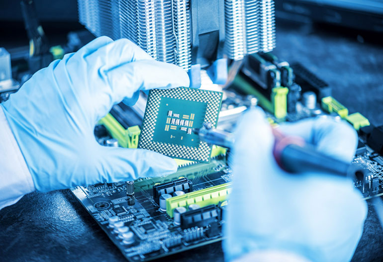
We leverage cutting-edge technologies to enhance production efficiency and reliability.

Learn more
post image

Your Partner in Semiconductor Innovation and Excellence

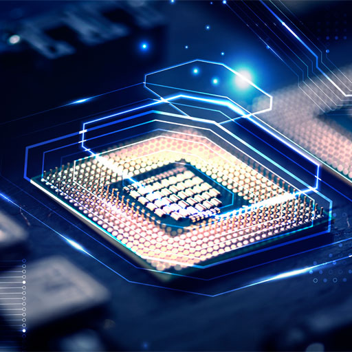
Join us in pioneering the future of semiconductor manufacturing in india.
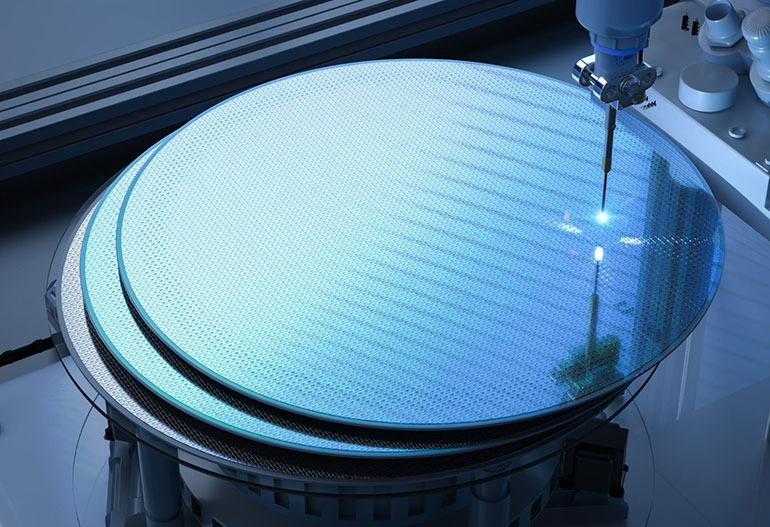
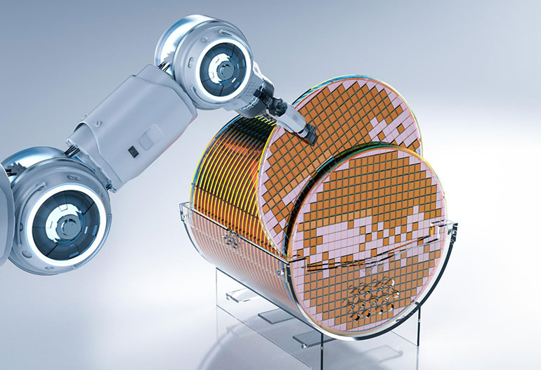
Learn more

Pioneering Semiconductor Manufacturing in India

Founded in 2023, QuadQuantum Pvt. Ltd. is on a mission to revolutionize India's tech landscape by establishing the nation's first semiconductor- grade silicon wafer manufacturing facility. Our vision is to empower the industry with cutting-edge 200mm and 300mm wafers, driving innovation and self-sufficiency.

about
about

Empower

Unlock the Future of Semiconductor Supply

Partnering with a local supplier of semiconductor-grade silicon wafers offers unmatched advantages. Enjoy cost savings, swift logistics, and assurance of quality that meets global standards.

Streamlined supply chain for enhanced operational efficiency.

Competitive pricing with reduced transportation costs.

Mitigate risks in a changing geopolitical landscape.

Learn more

Innovate

End-to-End Wafer Solutions

Transforming raw materials into high-quality semiconductor wafers.

Quality

Comprehensive Manufacturing Capabilities

From polysilicon to polished wafers, we deliver excellence.

post image

Precision

Advanced Wafer Types

Including SOI, Epitaxial, and compound semiconductor wafers.

post image

Innovation

Our Commitment

Delivering superior quality and compliance in every wafer.

post image

Engineering the Next Generation of Electronics, Photonics & Advanced Materials

2D Materials

2D materials are a cutting-edge class of crystalline materials consisting of one or a few layers of atoms. Their ultra-thin nature—combined with exceptional electrical, optical, mechanical, and thermal properties—makes them indispensable for the future of semiconductor and nanotechnology industries.

Since the revolutionary discovery of graphene, the library of 2D materials has expanded rapidly. Today, over 50 layered materials have been prepared in atomically thin form, including metals, semiconductors, insulators, topological materials, and superconductors.

  • Atomic-scale precision
  • Tunable bandgaps
  • High carrier mobility
  • Mechanical flexibility & transparency
  • Strong light-matter interaction
  • Compatibility with CMOS processing

These unique features open pathways toward ultra-fast, ultra-thin, ultra-efficient devices—ranging from transistors and optical sensors to flexible wearables and quantum systems.